
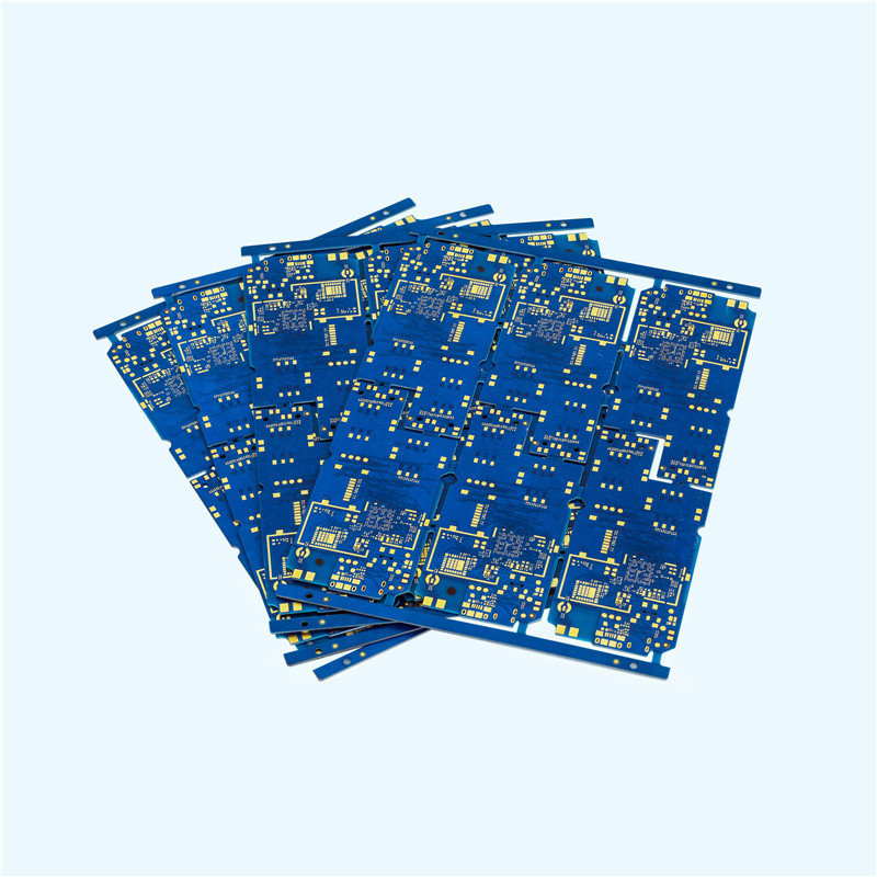
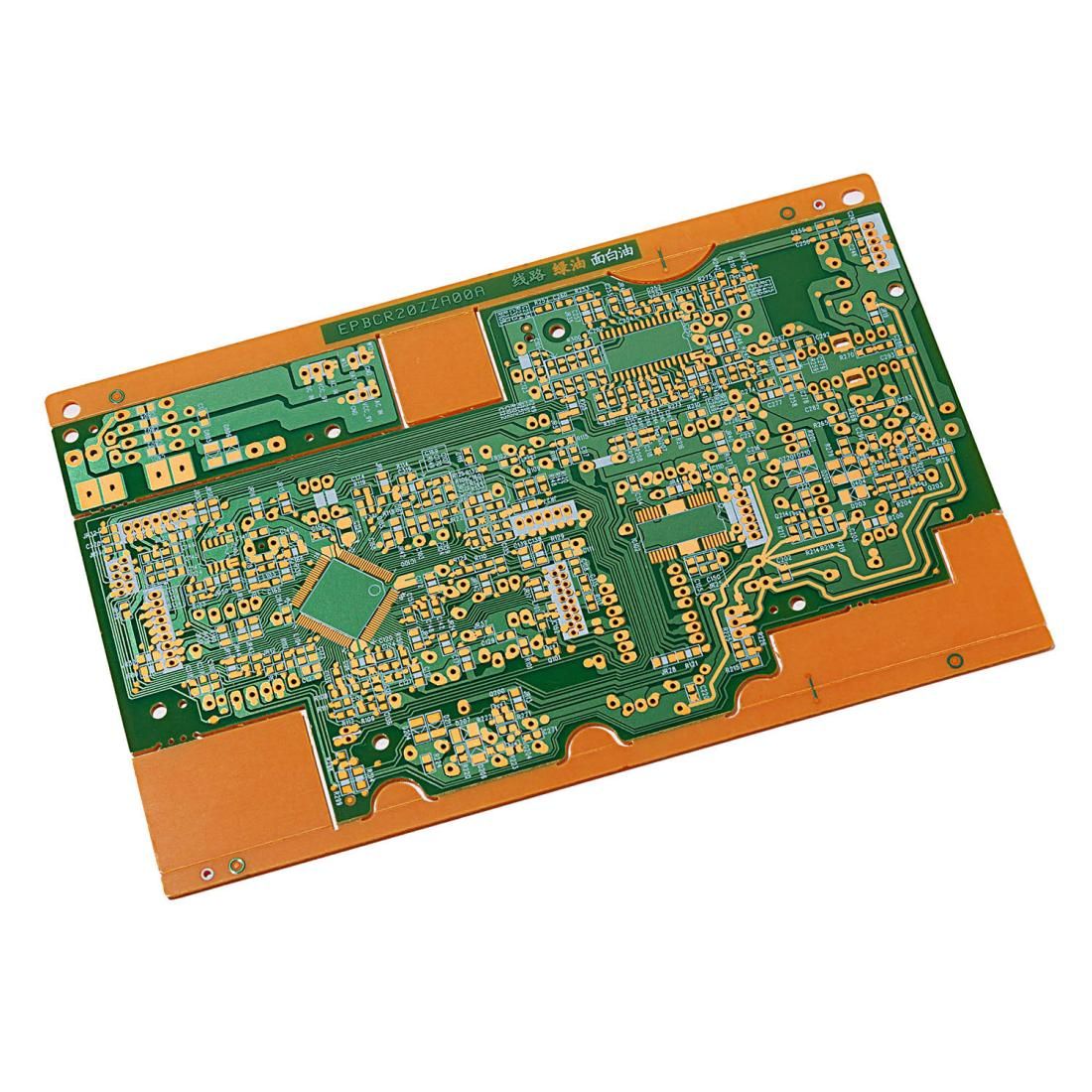
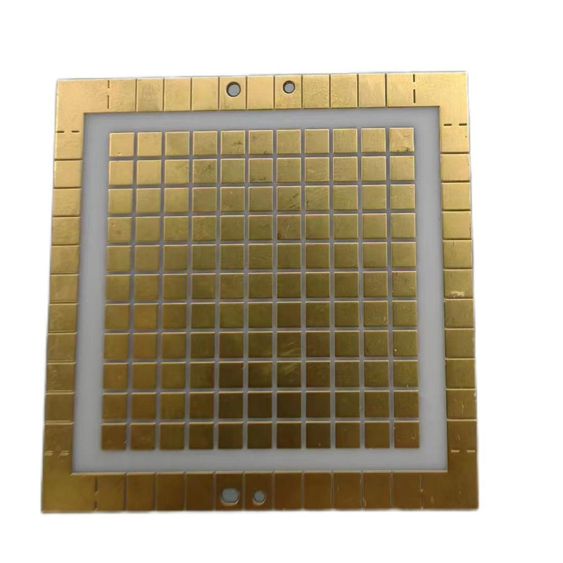


Multilayer Printed Circuit Boards
Characteristics of PCB Multilayer Board
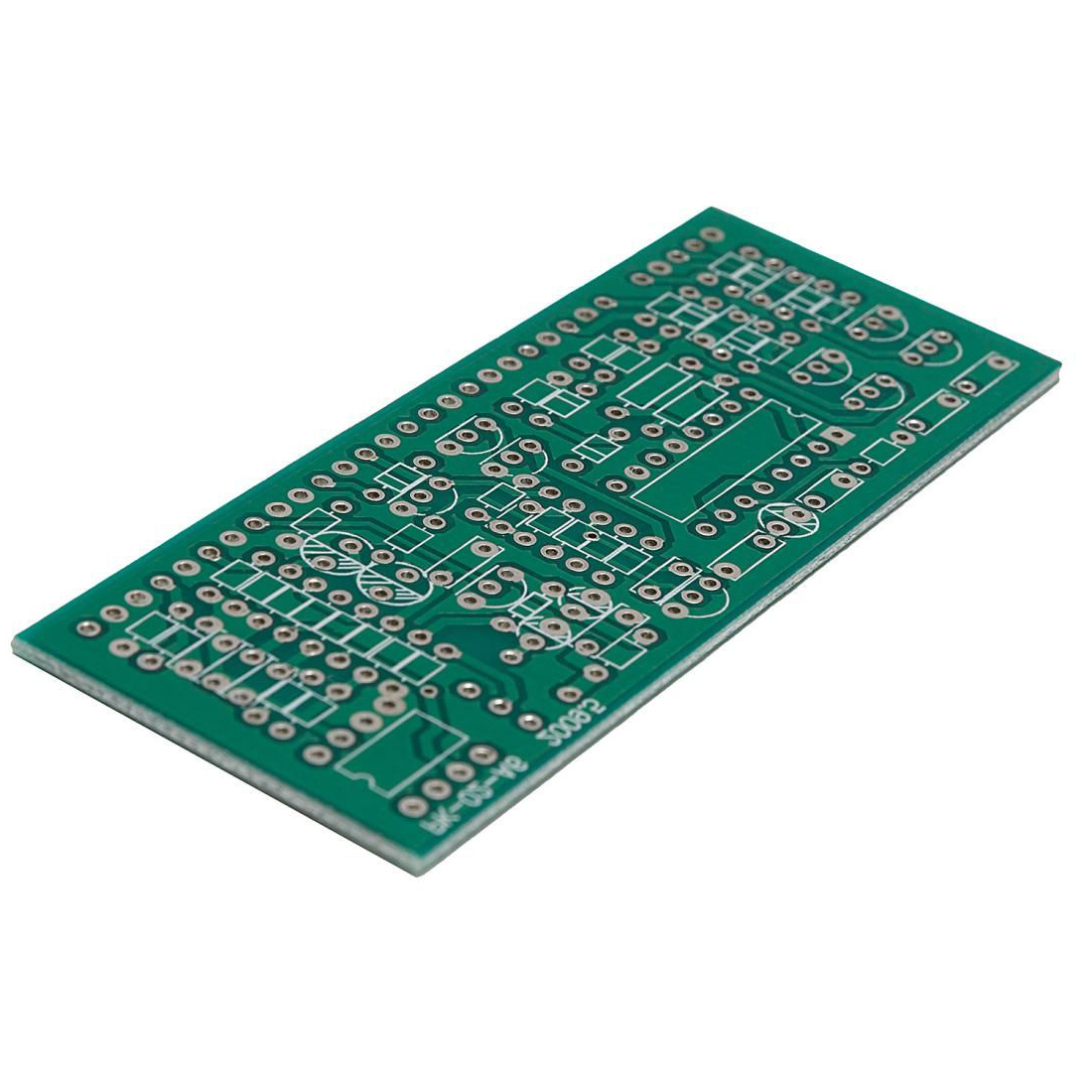
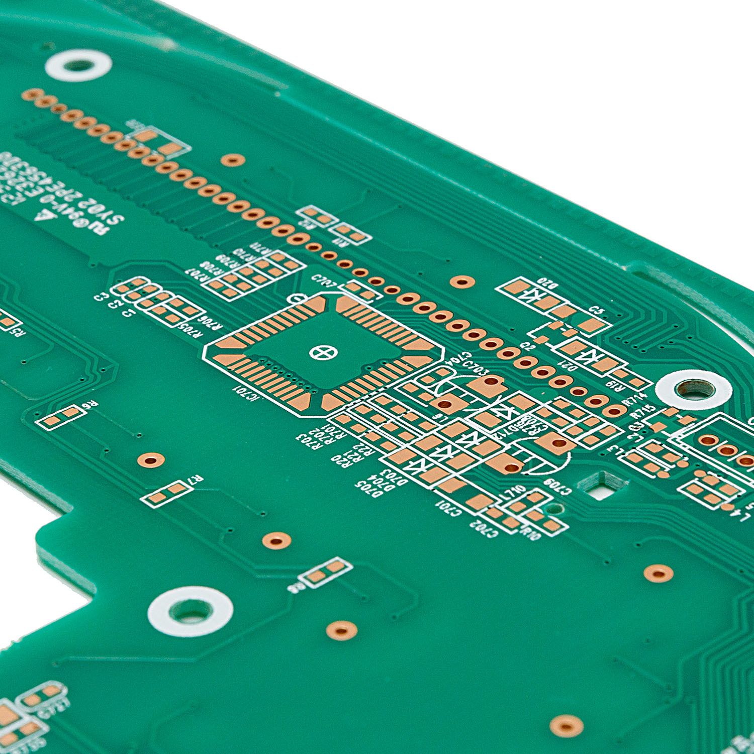
The biggest difference between a multi layer PCB board and a single or double panel is the addition of an internal power layer (maintaining the internal power layer) and a grounding layer. The power and ground network are mainly wired on the power layer. However, multi-layer board wiring is mainly based on the top and bottom layers, supplemented by the middle wiring layer. Therefore, the design method of multi-layer boards is basically the same as that of double-sided boards, and the key lies in how to optimize the wiring of the internal electrical layer to make the wiring of the circuit board more reasonable and have better electromagnetic compatibility.
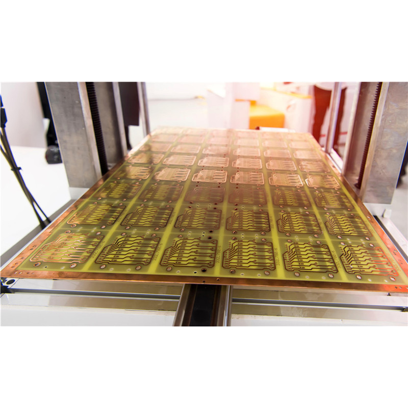
Process Flow of PCB Multilayer Board
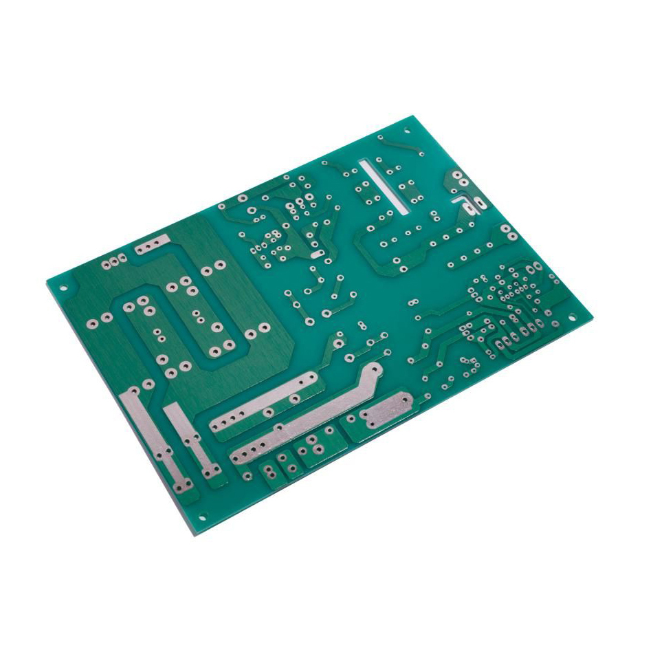
The difference between a double-sided PCB board and a single-sided PCB board is that the single panel circuit is only on one side of the PCB board, while the circuit of a double-sided PCB board can be connected between the two sides of the PCB board with a through hole in the middle.
product parameters
| Feature | AREX´s technical specification |
| Number of layers | 4 – 22 layers standard, 30 layers advanced, 40 layers prototype. |
| Technology highlights | Multiple layers of epoxy glass fiber bonded together with multiple layers of copper of varying thicknesses. |
| Materials | High performance FR4, halogen-free FR4, low loss and low Dk materials |
| Copper weights (finished) | 18μm – 210μm, advanced 1050μm / 30oz |
| Minimum track and gap | 0.075mm / 0.075mm |
| PCB thickness | 0.40mm – 7.0mm |
| Maxmimum dimensions | 580mm x 1080mm, advanced 610mm x 1400mm |
| Surface finishes available | HASL (SnPb), LF HASL (SnNiCu), OSP, ENIG, Immersion Tin, Immersion Silver, Electrolytic gold, Gold fingers |
| Minimum mechanical drill | 0.20mm |
| Minimum laser drill | 0.10mm standard, 0.075mm advanced |