
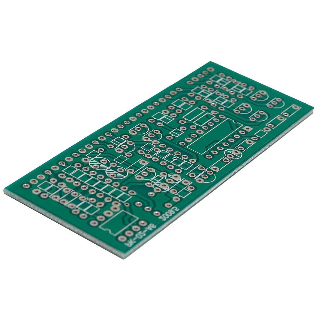
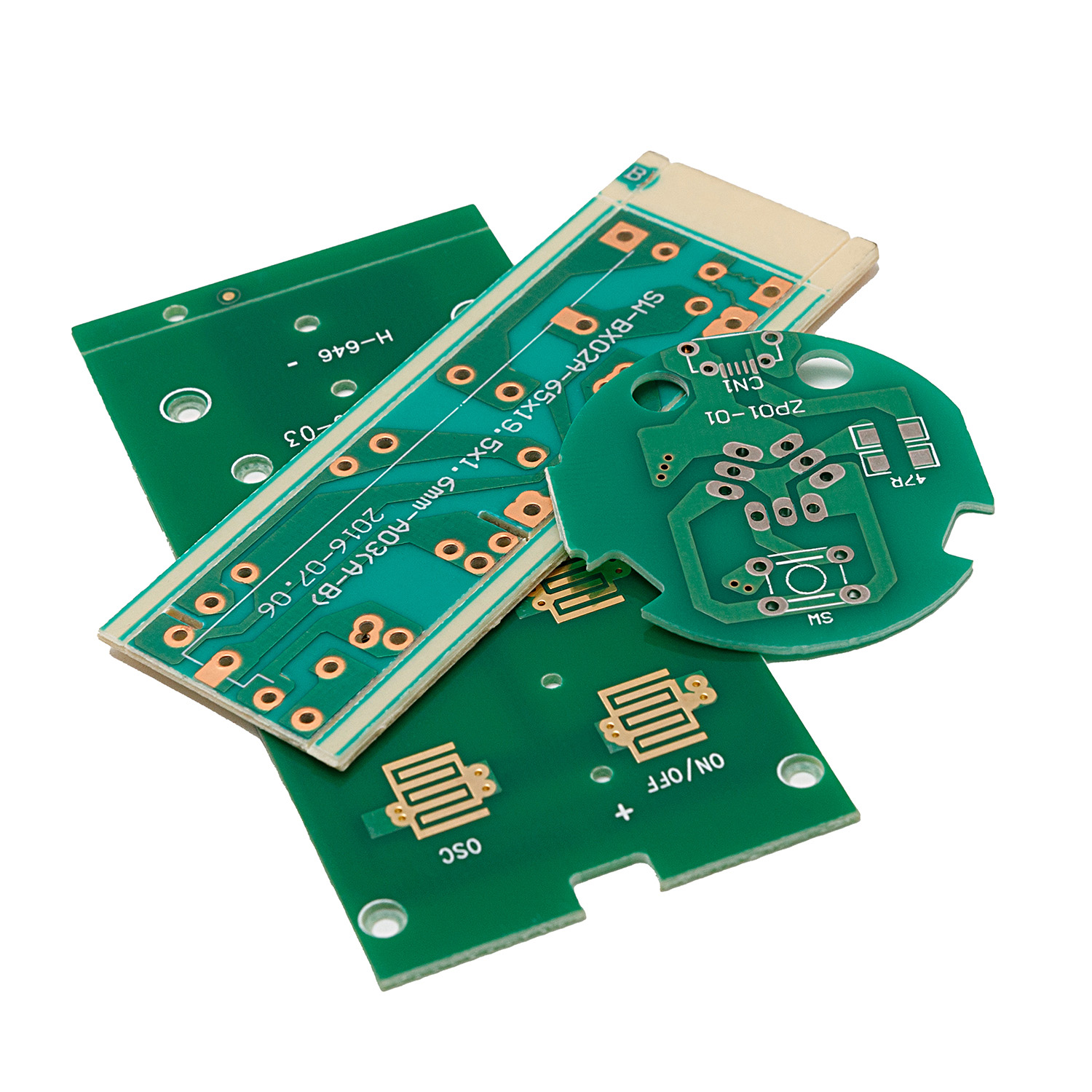
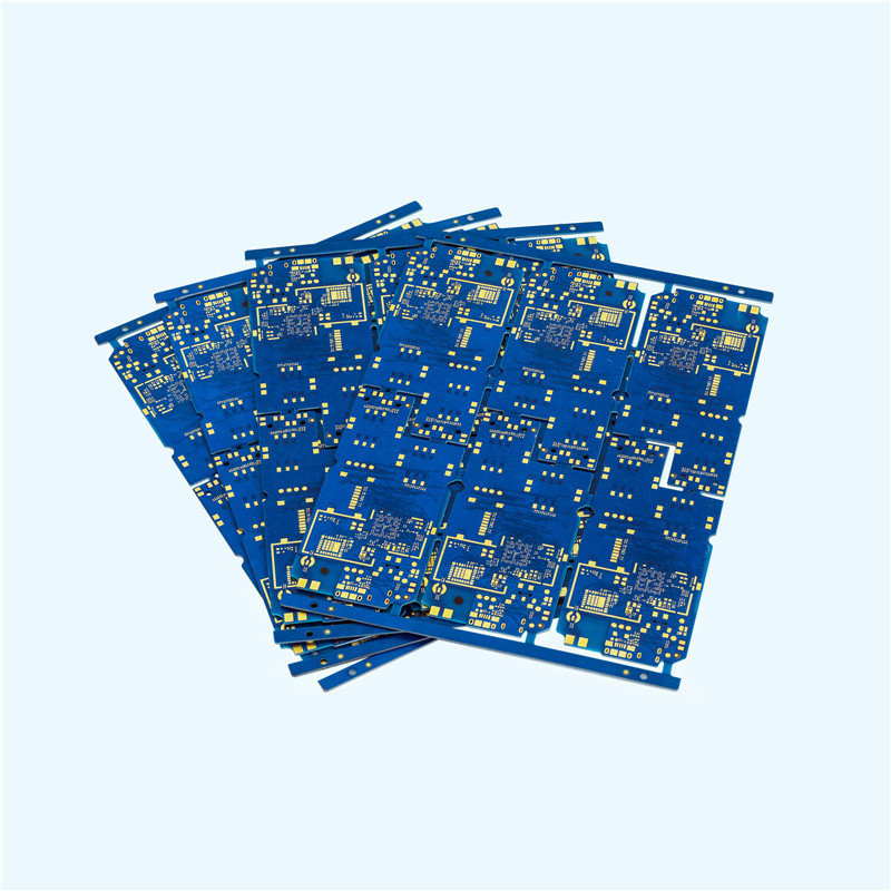
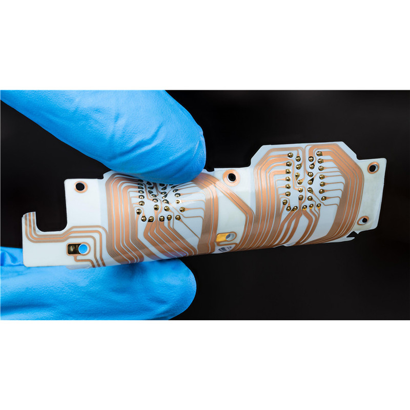
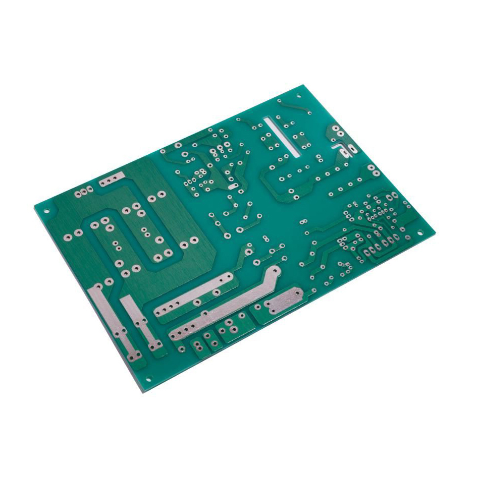
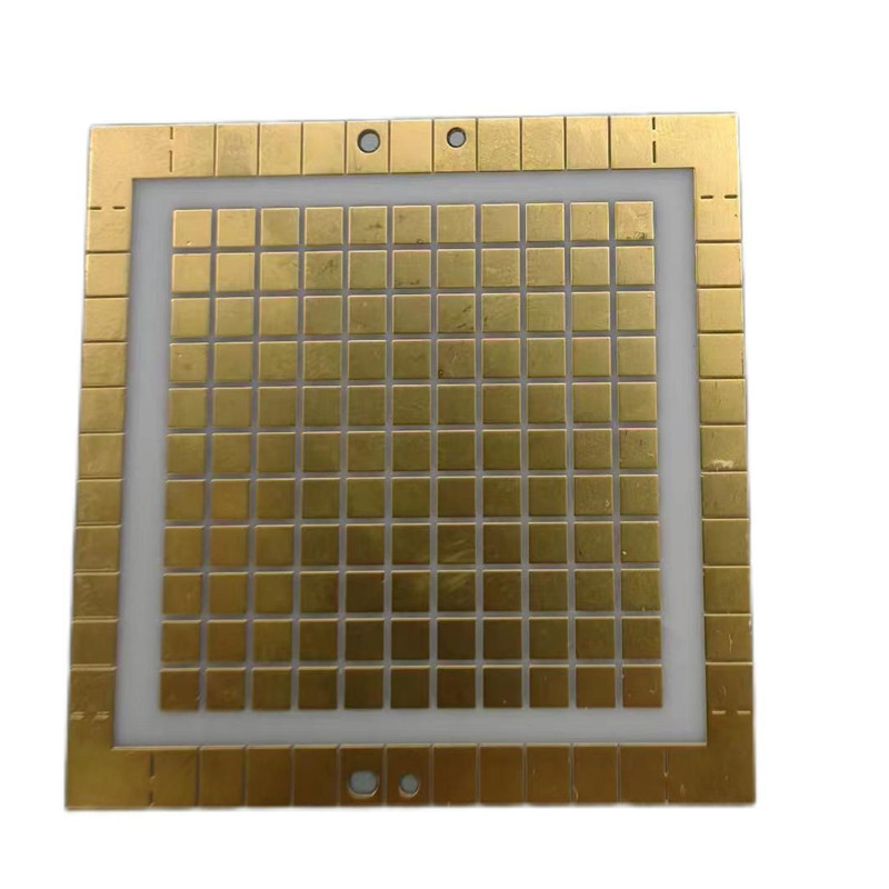
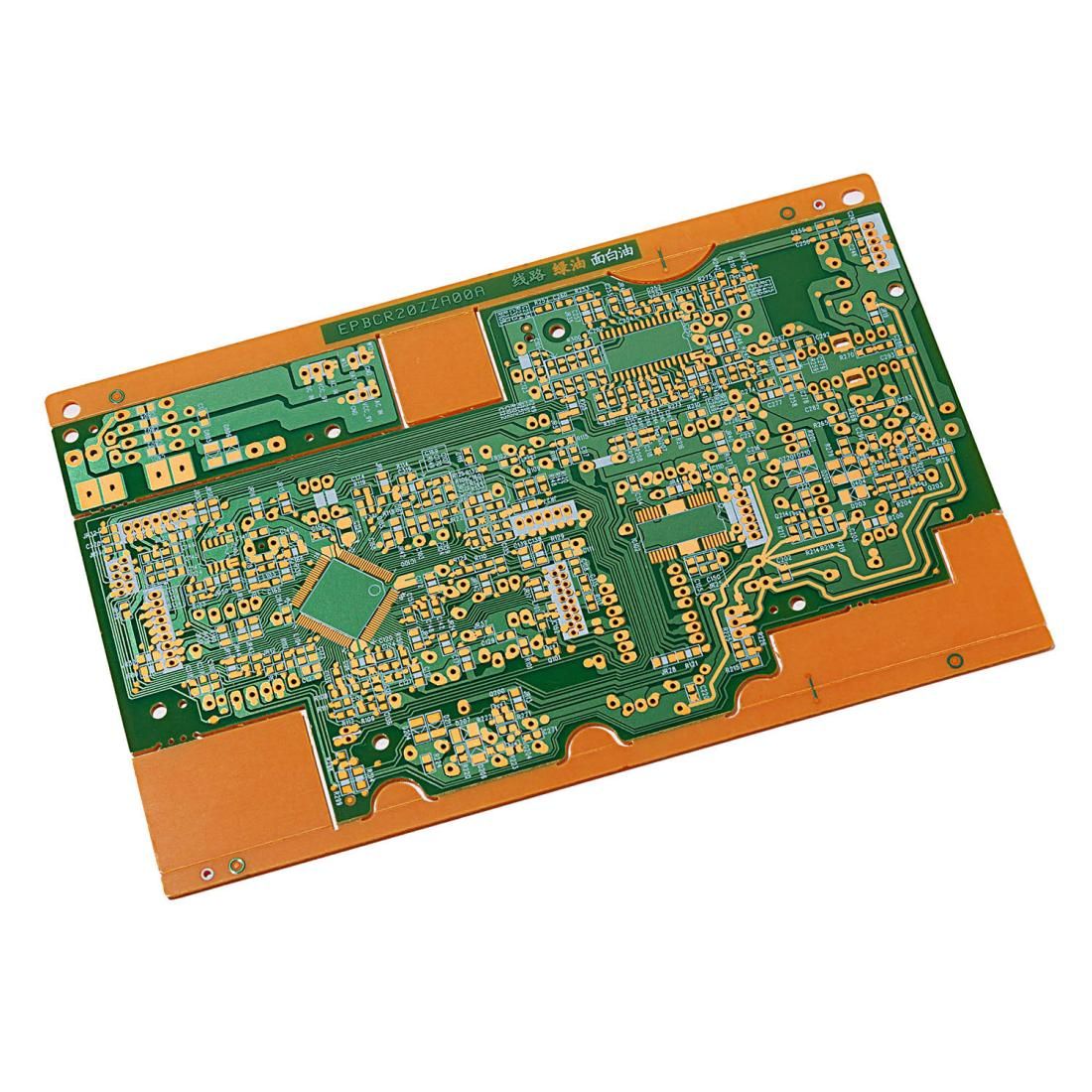

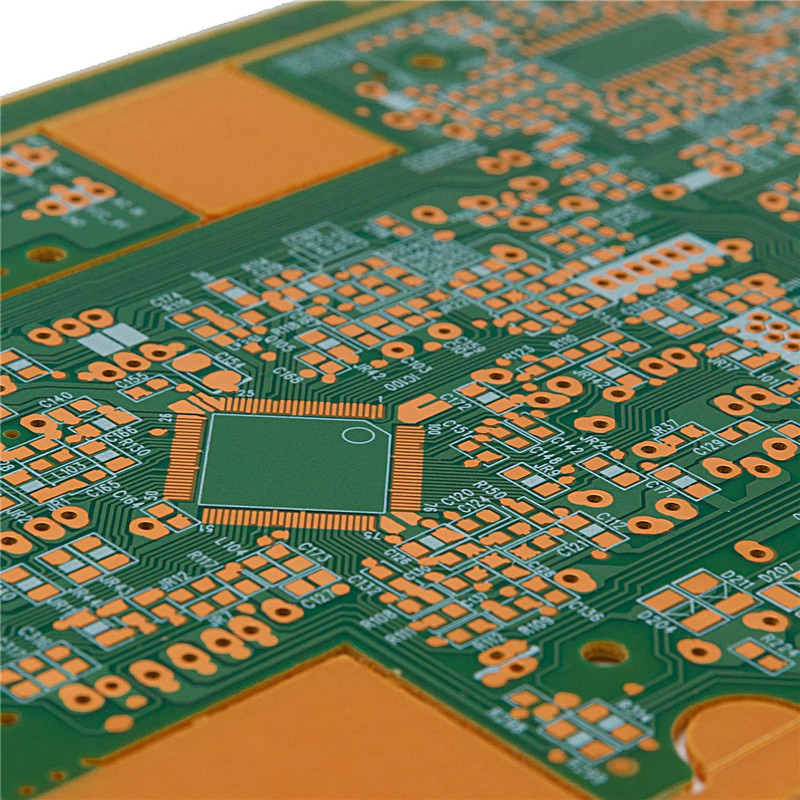
HDI PCB High Density Interconnect PCB
product introduction
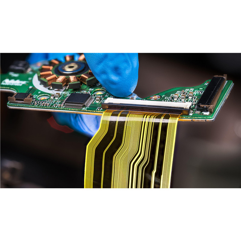
HDI PCB is suitable for products with crucial electrical performance and noise suppression. The advantages of HDI PCB include
HDI technology reduces the overall size of the product and improves electrical performance.
Strong impedance control and impressive high-frequency transmission capability
Application of HDI PCB Printed Circuit Board
● Power distributor
● Motor control
LED application control
● Satellites, micro systems
|
Feature |
AREX´s technical specification |
|
Number of layers |
4 – 22 layers standard, 30 layers advanced |
|
Technology highlights |
Multilayer boards with a higher connection pad density than standard boards, with finer lines/spaces, smaller via holes and capture pads allowing microvias to only penetrate select layers and also be placed in surface pads. |
|
HDI builds |
1+N+1, 2+N+2, 3+N+3,4+N+4, any layer / ELIC, Ultra HDI in R&D |
|
Materials |
FR4 standard, FR4 high performance, Halogen free FR4, Rogers |
|
Copper weights (finished) |
18μm – 70μm |
|
Minimum track and gap |
0.075mm / 0.075mm |
|
PCB thickness |
0.40mm – 3.20mm |
|
Maxmimum dimensions |
610mm x 450mm; dependant upon laser drilling machine |
|
Surface finishes available |
OSP, ENIG, Immersion tin, Immersion silver, Electrolytic gold, Gold fingers |
|
Minimum mechanical drill |
0.15mm |
|
Minimum laser drill |
0.10mm standard, 0.075mm advanced |